Configuration
J1: Target reset configuration
Jumper J1 connects the reset line and the target reset line. By default, J1 is populated.
When having problems establishing the initial debug session with the Emulation Adapter (EA), try to remove J1 and see if it makes any difference.
J2 and J3: Clock source configuration
Jumpers J2 and J3 select external clock source (XOSC) for the emulation device. Per default, both jumpers are set to position 1-2, which yields the external clock (XOSC) source being used from the Target board.
If an oscillator in the Target is not an option and the target crystal doesn’t oscillate in conjunction with the EA, the EA can also provide the external clock (XOSC) source by setting jumpers J2 and J3 in position 2-3. In this case, a crystal circuit must be built on the EA.
|
Note that the EA may not operate when crystal circuit is used in the target. Typical design guideline is that the crystal should be as close as possible to the microcontroller. It can happen that the target crystal does not oscillate in conjunction with the EA since clock lines (XTAL, EXTAL) between the target crystal and the emulation device on the EA become too long, inevitably too much affecting the impedance of the crystal circuit. If a “standalone” oscillator is used instead of the crystal circuit, no problems are expected. |

|
The crystal packed separately in the antistatic bag comes along the Emulation Adapter. It can be used to feed an external clock source (XOSC) to the emulation device by inserting the crystal into the Q1 socket. If a different clock frequency is required, use suitable crystal and insert it into the Q1 socket. The emulation adapters of revision A1 were delivered with a 40 MHz crystal, while the adapters of revision A2 or higher are delivered with a 20 MHz crystal. |
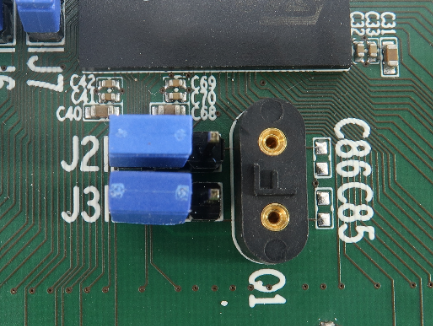
Crystal Q1 is located in the corner of the EA, next to the 38-pin Mictor connector P1 and per default not populated:
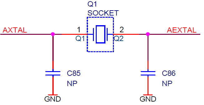
Capacitors C85 and C86, for which pads are provided on the EA PCB, are not populated since the microcontroller provides already the internal load capacitors for 40MHz crystal oscillator operation. |
J4 and J5: GND connecting points
|
|
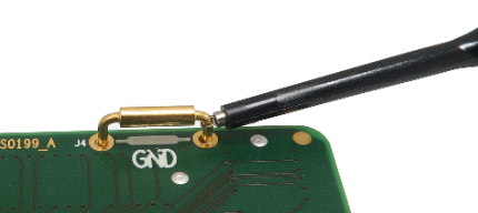
Real target microcontroller in the 176-pin package provides an exposed GND pad in the middle of the microcontroller at the bottom side of the package. This provides GND connection between the microcontroller and the target.
In case of the EA usage, the solder part is soldered instead of the microcontroller. Note that available solder parts until the introduction of this EA, haven't provided support for the exposed GND pad.
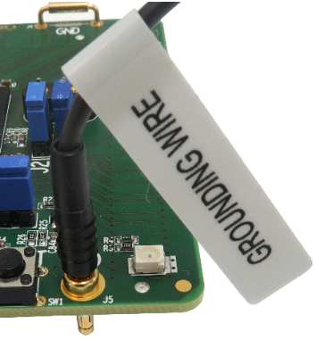
Ensure a replacement GND connection between the EA and the target using a dedicated GND wire. Without this connection, the system will not work. Use provided GND wire which comes along the EA and plug it to the pin J5 (see picture above) on the EA. Connect the other side to the ground potential on the target - as close as possible to the microcontroller respectively solder part being soldered instead of the microcontroller. This connection must be quality and reliable otherwise debugging and tracing over the Nexus trace port may not work. Alternatively, GND connection can be also established over the J4 ground bridge.
J6 and J7: RTC Clock source
Jumpers J6 and J7 select the RTC Clock source (32,768 kHz XTAL) for the emulation device. Per default, both jumpers are set to position 1-2, which yields the clock source being used from the target.
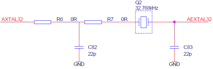
If an oscillator in the target is not an option and the target crystal doesn’t oscillate in conjunction with the EA, the EA can also provide the clock source (XTAL) by setting jumpers J6 and J7 in position 2-3. In this case, a crystal circuit must be built on the EA.
|
Note that the Emulation Adapter may not operate when crystal circuit is used in the target. Typical design guideline is that the crystal should be as close as possible to the microcontroller. It can happen that the target crystal does not oscillate in conjunction with the Emulation Adapter since clock lines (XTAL, EXTAL) between the target crystal and the emulation device on the Emulation Adapter become too long, inevitably too much affecting the impedance of the crystal circuit. If a “standalone” oscillator is used instead of the crystal circuit, no problems are expected. |
P2: Power supply configuration
Emulation Adapter Power supply is configured via the unshrouded 26-pin 2.54 mm header (P2).
Signal direction |
Signal |
Pin |
Pin |
Signal |
Signal direction |
|---|---|---|---|---|---|
Target |
TVDD_HV_OSC |
1 |
2 |
VDD_HV_OSC |
Emulation device |
Target |
TVDD_HV_ADR_S |
3 |
4 |
VDD_HV_ADR_S |
Emulation device |
Target |
VDD_HV_ADV_S |
5 |
6 |
VDD_HV_ADV_S |
Emulation device |
Target |
TVDD_HV_FLA |
7 |
8 |
VDD_HV_FLA |
Emulation device |
Target |
TVDD_HV_IO_MAIN |
9 |
10 |
VDD_HV_IO_MAIN |
Emulation device |
Target |
TVDD_HV_IO_ETH |
11 |
12 |
VDD_HV_IO_ETH |
Emulation device |
Target |
TVDD_HV_IO_EMMC |
13 |
14 |
VDD_HV_IO_EMMC |
Emulation device |
Not connected |
NC |
15 |
16 |
NC |
Not connected |
Not connected |
NC |
17 |
18 |
NC |
Not connected |
Not connected |
NC |
19 |
20 |
NC |
Not connected |
Ground |
GND |
21 |
22 |
GND |
Ground |
Ground |
GND |
23 |
24 |
GND |
Ground |
Ground |
GND |
25 |
26 |
KEY |
|
P2 Signal description
Refer to the microcontroller user’s manual for more details which power supply designation in the above table belongs to which power supply.
By default, all jumpers are set and connect target power supply coming from the target to the microcontroller residing on the Emulation Adapter. In principle, pins 1-2, 3-4, 5-6, 7-8, 9-10, 11-12 and 13-14 must be bridged only but for the convenience and ease of use all jumpers are set, except for pins 25-26. Pin 26 is the polarizer key preventing incorrect connection of the IEA-PS power supply, when being connected.
If a different power source is to be used (e.g., in case of a standalone operation), all jumpers must be removed and power source must be applied to:
•VDD_HV_OSC (pin 2), •VDD_HV_ADR_S (pin 4), •VDD_HV_ADV_S (pin 6), •VDD_HV_FLA (pin 8), |
•VDD_HV_IO_MAIN (pin 10), •VDD_HV_IO_ETH (pin 12), •VDD_HV_IO_EMMC (pin 14), •GND (pins 22, 24, 26) signals. |
The Emulation Adapter comes delivered together with the IEA-PS emulation adapter power supply, which simply plugs into the P2 header row, providing the necessary power supply for Emulation Adapter standalone operation. Double check that the power supply is configured properly for this particular Emulation Adapter.