PCB Design Guidelines
In this topic:
•Serial GigaBit Trace interfaces
•Serial GigaBit Trace interfaces
•Target connectors for Active Probe Infineon DAP/DAPE II
Introduction
This topic describes guidelines on how to design Printed Circuit Boards (PCB) to minimize high-frequency effects and to ensure the correct operation of the Serial GigaBit Trace interface.
Due to the continuously increasing demands of today’s embedded applications, MCUs get more and more complex by higher integration, flexible peripherals allocation, performance acceleration and power efficiency requirements. Upcoming multi-core processors impose even bigger challenges with increasing debug and trace interface speeds. However, physically all trace ports consist of several data lines and a clock. With higher integration and frequencies, the on-chip trace signals are subject to (increased) signal distortion which can prevent external hardware trace tool (e.g., BlueBox) from capturing the trace stream correctly.
The quality of on-chip trace signals depends mostly on the way how the debug interface is implemented by the semiconductor vendor but even more on the PCB layout design itself. To avoid signal distortion and to retrieve a high-quality trace already, the PCB designer should consider several aspects already to provide a stable environment.
Serial GigaBit Trace interfaces
Currently, we support:
•High Speed Serial Trace Port (HSSTP) on Arm devices
•Aurora Trace Port on:
oInfineon Aurix™ (AGBT, SGBT)
oNXP/ST Power Architecture®
oRenesas RH850
HSSTP interface runs at speeds up to 12.5 Gbps, whereas Aurora interface runs at speeds up to 5Gbps, which means high-speed board layout guidelines and practice must be considered while routing Serial GigaBit Trace physical interface from the transmitter (Target Board) to the receiver - trace tool (BlueBox).
Serial GigaBit Trace interface lines are connected directly to the FPGA implementing the physical interface. These lines exhibit the following characteristics:
Receive data lanes
To ensure interoperability between drivers and receivers of different vendors, AC coupling at the receiver input is used. 100nF AC coupling capacitors for connection to the transmitter are used at Aurora Nexus receiver input pins.
Transmit data lanes
This direction is normally not applicable for Aurora Nexus trace operation.
Clock lane
100nF AC coupling capacitors are located on the CLK output to protect drivers from possibly getting shorted. Target side usually has its own AC coupling.
Recommended measures
Following guidelines help minimizing high frequency effects and avoiding signal integrity issue:
Design concerns and placement
•For best signal integrity, CPU/MCU/SoC should be soldered directly on the PCB; any sockets in between might reduce the signal quality.
•Place debug/trace connector as close as possible to the CPU/MCU/SoC to minimize routing length.
•Ground signals should be soldered directly to the ground plane.
•Adjust termination to driver strength to match trace line impedance.
 Keep the trace line impedance at 50 Ohm. Place the termination resistor as close as possible to the driver.
•Any extra component on signals lines might reduce signal quality.
Minimize parasitic elements.
Debug/Trace lines routing
•Maintain the impedance.
•Lines should be routed as short as possible.
•Route over same reference layer (ground plane is preferred).
Review return signal path as well, since noise can occur on the reference plane as well.
•Lines length should be matched per specification.
Keep the same line length.
•Minimize amount of vias.
If minimizing is not possible, do not forget to return path vias.
•Consider potential crosstalk issues.
Keep away all trace lines from potential aggressor lines/signals and remove the trace clock from other signals by minimum 3 x width of it, because trace clock can act as aggressor.
•Design point to point connections with no stubs.
In case any stubs are needed, they should be as short as possible. If longer stubs are required, there should be a possibility to optionally disconnect them (e.g. by jumpers).
•Maintain the impedance for both single ended and differential signal lines.
•In case of differential signal lines keep the line length equal due to phase control.
Serial GigaBit Trace interfaces
•Preferred HSSTP/AGBT differential pair impedance is 100Ohm differential/50 Ohm single ended.
Maintain the impedance.
•Lines should be routed as short as possible.
•Traces should run on the same layer, or layers with the same impedance.
In case of changing routing layers add also return path vias.
•Samtec ERF8 connector ground pins should be connected directly to the PCB GND plane.
•Intra-pair length equal due to phase control.
•Use point to point connection.
Target connectors
Target connectors, also known as header connectors, are used to create connections between the embedded target and BlueBox Hardware (Active Probes, Debug Adapters, Active Probe Adapters etc.).
When designing your embedded target and selecting a target connector, it's essential to consider available space around the target connector to have a possibility to connect with BlueBox Hardware.
It’s recommended that you use standard target connectors. For more information regarding the target connector and compatibility with adapters, refer to Hardware User Manuals.
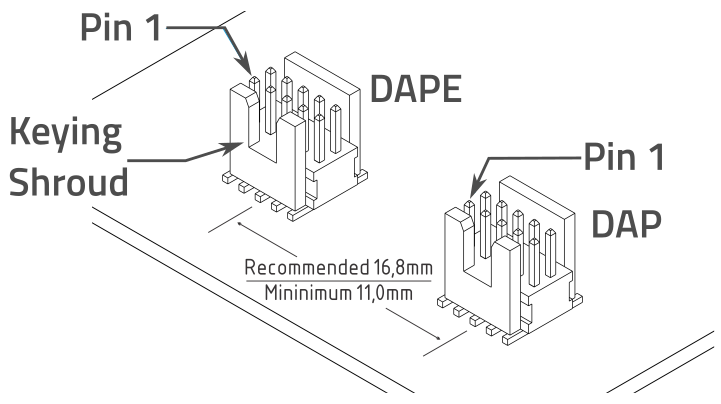
Target connectors for Active Probe Infineon DAP/DAPE II
The target debug connector is a 10-pin, 1.27mm, double-row connector (e.g. Samtec FTSH-105-01-L-DV,Samtec FTSH-105-01-L-DV-K with Keying Shroud).
1. Use the target debug connector(s) with the Keying Shroud option since incorrect connection can cause damage to the hardware.
2. Pin 1 of the connector(s) should be located toward the PCB’s edge to prevent the need to twist or fold the debug ribbon cable(s) (see the picture below).
3. When using DAP and the DAPE debug interfaces, the DAPE connector should be placed to the left of the DAP connector when looking from the edge of the PCB. The connectors must be at least 11.0 mm apart, although a distance of 16.8 mm is recommended. The goal should be to link the Active Probe to the target hardware via non-twisted and, when DAPE is used, parallel ribbon cables.